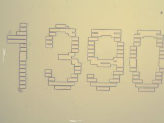
Large label written on an insulating substrate. Charging has caused the rectangles that make up the numbers to stitch together incorrectly, resulting in a broken look
Charging is what happens when electrons in the beam build up in your sample during exposure, creating an electric field that then distorts the beam and causes it to miss its targeted region. It's most common when writing on dielectric samples but has been observed to happen on almost every type of substrate. It can vary significantly from run to run; a job that didn't charge enough to be visible on one run can exhibit severe charging on the next one, due to variations in things like sample-stage contact area.
If you're seeing charging during a job, the most visible symptom will be a final, developed pattern that looks "broken"-- your shape is split into randomly separated/overlapping polygons. Charging can cause other odd effects but this is by far the most common in our system.
Luckily charging is relatively easy to deal with. There are a few different ways of approaching it, all of which involve putting some type of conductive layer on top of your resist film to allow the charge to dissipate.
Method 1: Metal films
The most obvious conductive film to use is any type of deposited metal, then strip the metal off after the write before the resist film is developed. Almost any type of metal film will work as long as the chemical used to strip it is compatible with your resist (e.g. don't use copper, as ammonium persulfate will chew up almost all organic resists). Gold is a good choice, since it strips easily in gold etch (KI) solution and can be quickly and easily deposited with the Cressington SEM sputter coater. Detailed process as follows:
Spin resist onto substrate and bake as needed
Sputter 2-3nm of gold onto the resist surface with the SEM sputter coater. 15-20 sec at the default setting will do this. The SEM sputterer is not meant for depositing thick films; please use the AJA sputterer if you need a coating thicker than a few nanometers!
Mount your sample on the relevant holder. Make sure you ground the sample surface to the stage using a copper grounding clip!
Run your e-beam job
Remove the gold with ~30sec of immersion in gold etch (found at the bottom of the acid/base cabinet or in a jar in the developer hood, typical etch rate is ~3 nm/sec). Overetching the gold won't hurt most samples. Gold etch can be rinsed away with DI water and disposed of in the labeled waste bottle under the development hood.
Develop your sample as usual.
Deposition method is important. Avoid using e-beam evaporation, as the x-rays produced will expose all types of e-beam resist. Thermal evaporation or sputtering both work well. Very little metal is needed; a thickness of 2-3 nm is plenty. Too much metal can cause the beam to scatter and broaden, resulting in larger-than-planned spot sizes.
Method 2: Metal films w/ sacrificial polymer
An easy way around the metal-stripping step above is to use a sacrificial water-soluble polymer between your resist and metal layer. That way the metal can be stripped by DI water immersion before the develop step. There's a commercial product called ESpacer for this, but it's ridiculously expensive. Luckily there is a good generic substitute based on poly(4-styrenesulfonic acid) (in a bottle labeled "FAKE E-SPACER" near the bay 5 resist). Process flow is as follows:
Spin resist
Spin fake espacer at 3krpm, bake at 90C for 3-5 mins
Deposit any metal (20sec of gold sputtering in the bay 5 SEM sputter coater gives a nice film)
Expose
Dissolve sacrificial layer in DI water. Metal will quickly lift off.
Develop as usual.
Since the polymer used in the espacer substitute is an acid, it isn't compatible with NEB31 or any other chemically-amplified resist. It works fine with PMMA, PMGI, ma-N 2403, and HSQ, however.
You can make your own fake e-spacer using poly(styrenesulfonic) acid (Sigma-Aldrich catalog number 561223) with ~1% surfactant added to improve water solubility. Triton X100 (Sigma-Aldrich catalog number X100) works well for this and is inexpensive. Thanks to Mike Rooks at Yale for the recipe!
Method 3: Conductive polymer
For the truly lazy, you can skip the metal entirely and spin a water-soluble conductive polymer on top of your resist. The commercial version of this is AquaSAVE?, which unfortunately is even more expensive than Espacer. One again though, we have a pretty good generic version in the lab (bottle of 1% PSS:PEDOT labeled "Aquasave" near the resist). Process flow:
Spin resist
Spin fake aquasave at 2-3krpm, bake 90C for 3-5mins
Expose
Dissolve aquasave in DI water for 1-2 mins
Develop as usual
It should be noted that there are some problems with this method. The PSS:PEDOT copolymer that the fake aquasave is based on can get crosslinked with certain resists during exposure; it only really works well with PMMA or PMMA/PMGI bilayers and then only if the dose isn't too high (<1000uC/cm2). It also isn't nearly as conductive as metal, so aquasave or its generic counterpart may not help you if the charging you're experiencing is very severe. It can't be beat for speed and ease of use though.
If you'd like to make your own fake Aquasave, use "conductive" grade PSS:PEDOT (Sigma-Aldrich catalog number 483095). You can add a small amount (~1%) of surfactant ( Triton X100 is good) to improve the solubility somewhat. Avoid the "high-conductivity" grade, as it isn't very water-soluble after spinning, baking, and exposure.
In all of these cases, all the charge-suppression material in the world won't help you if you don't ground the conductive film with one of the grounding clips on the Vistec's stage, so don't forget to do that.